InfiniteHBD: Building Datacenter-Scale High-Bandwidth Domain for LLM with Optical Circuit Switching TransceiversInfiniteHBD:以光路交換光模組為 LLM 打造資料中心規模的高頻寬域
After reading, you can explain why switch-based scale-up domains stay small and fragment under faults, and how a switch inside each transceiver builds rings of any size around failed nodes.讀完後,你能說明為什麼以交換器為核心的 scale-up 域規模有限、遇到故障會碎片化,以及光模組內的開關如何繞過故障節點,組出任意大小的環。
A high-bandwidth domain (HBD) is the scale-up network, such as NVLink, that gives each GPU terabits per second for tensor parallelism. Switch-based HBDs such as NVL-72 are costly, so they stay small, and when the TP size does not divide a domain's healthy GPUs, the remainder sits idle. Switchless GPU rings are cheap, but one failed GPU breaks them. InfiniteHBD puts a small silicon-photonic switch inside each 800G transceiver: the light goes to one of two fibres or loops back inside the node. Nodes are wired to neighbours up to hops away, so loopback closes a ring of any size and a backup fibre skips a failed node. Measured: the prototype switches in 60–80 µs, loses 3.3 dB on average, and its switch draws about 3.2 W in a module under 12 W; a 32-GPU fixed-optics ring reached 77.1–77.3% of ring bandwidth in AllReduce, against 81.8% for an H100 server without SHARP; a 348-day production trace shows 2.33% of nodes faulty on average and 7.22% at p99. The headline waste and MFU gains are simulation.
高頻寬域(HBD)就是 scale-up 網路,例如 NVLink,給每顆 GPU 每秒數 Tb 來跑張量平行。NVL-72 這類以交換器為核心的 HBD 很貴,所以規模有限;當 TP 大小無法整除一個域內健康 GPU 的數量時,餘數就閒置。沒有交換器的 GPU 環很便宜,但壞一顆 GPU 就斷。InfiniteHBD 在每個 800G 光模組裡放進一個小型矽光子開關:光可以走兩條光纖之一,或在節點內迴環。節點接到 跳以內的鄰居,所以迴環能閉合任意大小的環,備援光纖能跳過故障節點。實測:原型切換需 60–80 µs、平均損耗 3.3 dB,開關約耗 3.2 W,整個模組低於 12 W;用固定光模組接成的 32-GPU 環在 AllReduce 中用到環頻寬的 77.1–77.3%,未啟用 SHARP 的 H100 伺服器是 81.8%;348 天的生產故障紀錄顯示平均 2.33%、p99 7.22% 的節點故障。標題上的浪費與 MFU 增益來自模擬。
1. Where this paper sits1. 這篇論文的位置
The Chapter 2 describes a ladder of links (§01 and its first panel). Tensor parallelism (TP) stays on the top network rung, NVLink, because its collectives sit inside every layer; §02 draws that rung as eight GPUs on one NVSwitch fabric. Such a fabric is a high-bandwidth domain (HBD), or scale-up domain: the GPUs that reach each other at terabits per second. All other traffic uses the NICs, one rung down, so the size of the HBD caps the size of a TP group. §05 treats a transceiver as a fixed point-to-point part that costs money, draws power and fails. This paper turns it into a small switch.
第 2 章描述了一道鏈路階梯(§01 與它的第一個面板)。張量平行(TP)留在網路的最上階 NVLink,因為它的集體操作位於每一層內部;§02 把這一階畫成八顆 GPU 共用一個 NVSwitch 互連。這樣的互連就是高頻寬域(HBD),也叫 scale-up 域:彼此能以每秒數 Tb 互通的那群 GPU。其餘流量都走往下一階的 NIC,所以 HBD 的大小限制了 TP 群組的大小。§05 把光模組當成固定的點對點零件:要花錢、耗電、會壞。這篇論文把它變成一個小交換器。
The Chapter 6, §5, shows an older optical answer: TPU v4 joins 64-chip cubes through 48 central MEMS optical circuit switches (OCS), which move mirrors in milliseconds. A fault there still costs a cube. The paper sorts existing HBDs into three families. Each has one weak point, measured by the fault explosion radius: the number of GPUs that one fault degrades.
第 6.9 節 介紹了較早的光學答案:TPU v4 透過 48 台集中式 MEMS 光路交換器(OCS)連接 64 顆晶片的 cube,鏡面轉動需要毫秒。在那裡,一次故障仍要賠上一個 cube。論文把現有的 HBD 分成三個家族,各有一個弱點,用故障爆炸半徑衡量:一次故障拖累的 GPU 數量。
| Family | 家族 | Examples | 例子 | Weak point | 弱點 | Fault radius | 故障半徑 |
|---|---|---|---|---|---|---|---|
| Switch-centric | 以交換器為核心 | NVL-36 / 72 / 576 | Switch chips are costly, so domains stay small and fragment | 交換晶片昂貴,域小且會碎片化 | A node; a failed switch degrades every GPU on it | 一個節點;交換器故障會拖累接在它上面的所有 GPU | |
| GPU-centric | 以 GPU 為核心 | TPUv3, Dojo, SiP-Ring | GPUs forward traffic; one failure breaks the ring or mesh | GPU 轉送流量;壞一顆,環或網格就斷 | The whole HBD | 整個 HBD | |
| Switch–GPU hybrid | 交換器與 GPU 混合 | TPUv4, TPUv5p | Central OCS between cubes; port count limits scale | cube 之間用集中式 OCS;埠數限制規模 | One 64-chip cube | 一個 64 顆晶片的 cube | |
| Transceiver-centric | 以光模組為核心 | InfiniteHBD | Ring collectives only | 只支援環狀集體操作 | One node | 一個節點 |
2. The problem, measured2. 問題,用量測說話
Fragmentation. A TP group needs exactly healthy GPUs inside one HBD. If a domain of GPUs has failed GPUs, and does not divide by , the remainder cannot join any group. The paper writes the waste ratio of one HBD as
碎片化。一個 TP 群組需要在同一個 HBD 內湊滿 顆健康 GPU。若一個有 顆 GPU 的域壞了 顆,而 不能被 整除,餘數就無法加入任何群組。論文把單一 HBD 的浪費比例寫成
The paper's own examples, and the same rule for NVL-36 and NVL-72 with no failure, one question per row:
論文自己的例子,以及同一規則套在沒有故障的 NVL-36 與 NVL-72,逐列計算如下:
| Question問題 | Calculation算式 | Result結果 |
|---|---|---|
| Two 32-GPU HBDs, one failed GPU each, TP-16兩個 32-GPU HBD,各壞一顆,TP-16 | idle GPUs顆閒置 | |
| One 64-GPU HBD, two failed GPUs, TP-16一個 64-GPU HBD,壞兩顆,TP-16 | idle GPUs顆閒置 | |
| NVL-36, no failure, TP-16NVL-36,沒有故障,TP-16 | ||
| NVL-72, no failure, TP-32NVL-72,沒有故障,TP-32 | one GPU in nine九顆中一顆 |
A bigger domain wastes less for the same faults, because each domain leaves only one remainder. The 1/9 in the last row is the share that the paper says NVL-36 and NVL-72 hold back at TP-16 and above. The figure below draws the first two rows.
同樣的故障,較大的域浪費較少,因為每個域只留下一份餘數。最後一列的 1/9,就是論文所說 NVL-36 與 NVL-72 在 TP-16 以上時保留下來的比例。下圖畫出前兩列。
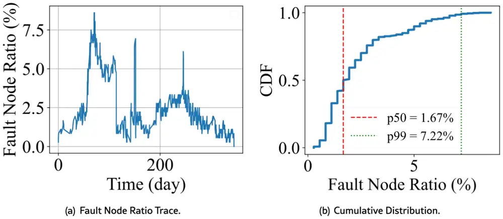
How often nodes fail. The authors logged every fault in a pretraining cluster of about 3K GPUs in 8-GPU nodes for 348 days, with start time, end time and node ID (Appendix A; the trace is open source). On average 2.33% of the nodes were faulty at any moment. The median was 1.67% and the 99th percentile 7.22%. For the 3,200 GPUs of the trace (§7), the arithmetic is:
節點多常故障。作者記錄了一個約 3K 顆 GPU、8-GPU 節點的預訓練叢集在 348 天內的每一次故障,包括開始時間、結束時間與節點 ID(附錄 A;這份紀錄已開源)。任一時刻平均有 2.33% 的節點故障,中位數 1.67%,第 99 百分位 7.22%。以紀錄中的 3,200 顆 GPU(§7)計算:
| Question問題 | Calculation算式 | Result結果 |
|---|---|---|
| Faulty nodes at the mean (400 nodes)平均時的故障節點(400 個節點) | nodes個節點 | |
| Faulty nodes at p99p99 時的故障節點 | nodes個節點 | |
| Per-GPU fault probability , from 每顆 GPU 的故障機率 ,由 反推 | ||
| The same rate for a 4-GPU node (half the GPUs)換算成 4-GPU 節點的故障率(GPU 數減半) |
The last two rows are the paper's conversion, which assumes independent GPU faults. So a cluster always has a handful of dead nodes, and in bad weeks a few dozen.
最後兩列是論文的換算,假設 GPU 故障彼此獨立。所以一個叢集隨時都有幾個死掉的節點,糟糕的幾週則有好幾十個。
Two lessons follow. The unit of loss should be one node, not a ring, a cube or a domain. And the domain should be large, so that one remainder is small against it.
由此得到兩個教訓。損失的單位應該是一個節點,而不是一個環、一個 cube 或一個域。而且域要大,讓一份餘數相對於它很小。
3. The design3. 設計
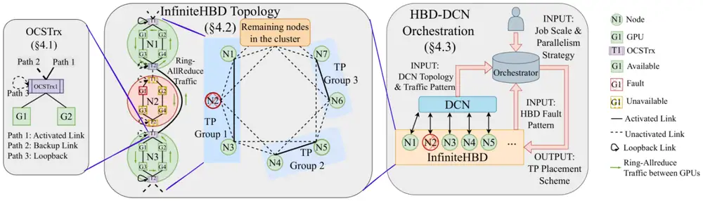
InfiniteHBD has three parts: a switching transceiver, a ring topology built from it, and an orchestrator that places TP groups so that the datacenter network (DCN) also stays quiet. Figure 2 of the paper shows all three.
InfiniteHBD 有三個部分:會切換的光模組、用它搭成的環狀拓樸,以及一個擺放 TP 群組、同時讓資料中心網路(DCN)保持安靜的編排器。論文的 Figure 2 畫出這三者。
3.1 An optical switch inside the transceiver3.1 光模組裡的光開關
OCSTrx is a QSFP-DD 800 Gb/s transceiver with an optical circuit switch on its photonic chip. A linear driver and modulators put the GPU's electrical lanes onto light from one laser. The light then enters a switch built from Mach–Zehnder interferometers (MZI). An MZI splits light into two arms; a heater changes the phase in one arm (the thermo-optic effect), and interference at the output sends the light to one port or the other. Two MZI elements choose among three paths: path 1 to the main fibre, path 2 to the backup fibre, and path 3, a loopback inside the module. A small MZI matrix steers the loopback from the upper half of the lanes to the lower half, so the signal returns on the other GPU's lanes. The receiver has one photodetector per path.
OCSTrx 是一個在光子晶片上整合了光路開關的 QSFP-DD 800 Gb/s 光模組。線性驅動器與調變器把 GPU 的電訊號 lane 調到一顆雷射的光上。接著光進入以馬赫–曾德干涉儀(MZI)構成的開關。MZI 把光分成兩臂;加熱器改變其中一臂的相位(熱光效應),輸出端的干涉就把光送到其中一個埠。兩個 MZI 元件在三條路徑中選一條:路徑 1 通往主光纖,路徑 2 通往備援光纖,路徑 3 是模組內的迴環。一個小型 MZI 矩陣把迴環從上半部 lane 導到下半部 lane,讓訊號從另一顆 GPU 的 lane 回去。接收端每條路徑有一個光偵測器。
Two choices keep it cheap. First, the whole bandwidth goes to one path at a time: turning one external path on turns the other off, so bandwidth is never split. Second, the switch has only three outputs. MEMS mirror switches reach 320 × 320 ports but take milliseconds and cost more. A silicon-photonic switch loses light at every stage, which limits its radix, but three outputs need very few stages. A failed OCSTrx looks like an ordinary failed transceiver.
兩個選擇讓它便宜。第一,同一時間全部頻寬只給一條路徑:開啟一條外部路徑就會關閉另一條,所以頻寬從不分割。第二,開關只有三個出口。MEMS 鏡面開關可達 320 × 320 埠,但需要毫秒且較貴。矽光子開關每經過一級就損失一些光,限制了它的埠數;但三個出口只需要很少的級數。OCSTrx 故障時,看起來就像一個普通的光模組故障。
3.2 The K-hop ring3.2 K 跳環
Inside a node. A node with GPUs carries bundles of OCSTrx. A bundle is several modules, for example 8 × 800 Gb/s for a GPU with 6.4 Tb/s of scale-up bandwidth. Each bundle serves a pair of GPUs, one on the upper half of the lanes and one on the lower half. Put nodes in a line and switch the two end bundles to loopback: traffic runs out on one half and back on the other, so all GPUs of the line form one ring. Any number of nodes can be closed this way, so the TP size is chosen at job start, not fixed by cables.
節點內。有 顆 GPU 的節點配 組 OCSTrx。一組包含好幾個模組,例如給有 6.4 Tb/s scale-up 頻寬的 GPU 用 8 × 800 Gb/s。每一組服務一對 GPU,一顆接上半部 lane、一顆接下半部 lane。把節點排成一條線,兩端的那一組切到迴環:流量沿一半出去、沿另一半回來,整條線上的 GPU 就形成一個環。用這種方式可以閉合任意數量的節點,所以 TP 大小在任務開始時選定,而不是由線纜決定。
Between nodes. Each node links to the nodes at (), so it has links. Ring AllReduce needs only a predecessor and a successor, so two links are active and are backups. If N4 fails, N3 and N5 switch their transceivers to the backup fibre between them, and only N4 leaves the ring. A run of up to failed nodes is bridged the same way; only a run of or more cuts the line. This pruned mesh works because ring traffic goes only to neighbours and node failures are mostly independent, so long runs are rare. Links and cost grow linearly with the number of nodes.
節點之間。每個節點連到 位置的節點(),所以有 條鏈路。環狀 AllReduce 只需要一個前驅和一個後繼,所以兩條鏈路啟用、 條作為備援。若 N4 故障,N3 與 N5 把光模組切到它們之間的備援光纖,只有 N4 離開環。連續至多 個故障節點都能用同樣方式橋接;只有連續 個以上才會切斷這條線。這種修剪過的網格行得通,是因為環的流量只到鄰居,而節點故障大多彼此獨立,長串連續故障很少見。鏈路數與成本隨節點數線性成長。
The waste bound. Appendix C bounds the extra waste that cuts cause. A cut inside a TP group of GPUs wastes at most GPUs. A middle node sees about cuts on average, where is the node failure probability. Summed over the line, the expected waste ratio is
浪費的上限。附錄 C 為切斷造成的額外浪費給出上限。在 顆 GPU 的 TP 群組內部切斷一次,最多浪費 顆 GPU。中間的節點平均看到約 個切斷點, 是節點故障機率。加總整條線,期望浪費比例為
With the trace's p99 rate (7.22% for 8-GPU nodes; 3.67% for 4-GPU nodes by the same conversion) and TP-32, the paper's Table 7 follows. We recomputed every entry:
代入紀錄中的 p99 故障率(8-GPU 節點 7.22%;以同樣換算,4-GPU 節點 3.67%)與 TP-32,就得到論文的 Table 7。我們重算了每一格:
| Node size and hops節點大小與跳數 | Calculation算式 | Result結果 |
|---|---|---|
| , , | ||
| , , | ||
| , , | Table 7 prints it as a fraction, Table 7 以分數印出: | |
| , , | ||
| , , | ||
| , , |
Each extra hop multiplies the bound by . The paper calls nearly negligible. That holds for 4-GPU nodes (0.28%); 8-GPU nodes need to reach 0.13%. This is analysis at the p99 rate, not a measurement. The panel below lets you cut a ring yourself.
每多一跳,上限就乘上一次 。論文說 幾乎可以忽略。這對 4-GPU 節點成立(0.28%);8-GPU 節點要 才降到 0.13%。這是以 p99 故障率做的分析,不是量測。下面的面板讓你自己切斷一個環。
Press the p99 preset and set . Find the smallest at which the ring wastes less than 1%, and compare it with the bound. Then look at the static TP rings: why does their waste not depend on at all, and what does that say about where the fault radius comes from?
按下 p99 預設值並設 。找出讓環的浪費低於 1% 的最小 ,再和上限比較。接著看靜態 TP 環:為什麼它們的浪費完全不受 影響?這說明故障半徑是從哪裡來的?
3.3 Placing TP groups so the DCN stays quiet3.3 擺放 TP 群組,讓 DCN 保持安靜
Data, pipeline and context parallelism (DP, PP, CP) still cross the DCN. If the HBD links nodes in deployment order, a TP group fills one ToR, and the DP peers of its GPUs sit under other ToRs, so DP traffic crosses the congested upper tiers. InfiniteHBD wires the HBD the other way. With nodes per ToR, node gets main links to and backups to , so its HBD neighbours sit under the next ToR. Nodes with the same index under every ToR form a parallel sub-line. TP groups run along a sub-line, across ToRs on the HBD, and the CP or DP peers of each GPU stay under one ToR.
資料、管線與上下文平行(DP、PP、CP)仍要跨越 DCN。如果 HBD 依部署順序連接節點,一個 TP 群組就填滿一台 ToR,而它的 GPU 的 DP 夥伴在其他 ToR 之下,所以 DP 流量要穿過壅塞的上層。InfiniteHBD 反過來接 HBD。每台 ToR 下有 個節點時,節點 的主鏈路接到 ,備援接到 ,所以它的 HBD 鄰居在下一台 ToR 之下。每台 ToR 下同一編號的節點組成一條平行子線。TP 群組沿子線經 HBD 跨越 ToR,而每顆 GPU 的 CP 或 DP 夥伴留在同一台 ToR 之下。
At run time the orchestrator drops faulty nodes, finds the connected healthy pieces by depth-first search, and cuts TP groups in order, in time for nodes. On a Fat-Tree, a TP group should also stay inside one aggregation-switch domain, and TP groups on parallel sub-lines should be aligned so that CP stays under the ToRs. Alignment has a price: one failed node then removes its whole ToR row, which multiplies the fault radius by the nodes per ToR. A binary search finds the strictest rule set under which the job still fits, in .
執行時,編排器剔除故障節點,以深度優先搜尋找出相連的健康片段,再依序切出 TP 群組,對 個節點的時間是 。在 Fat-Tree 上,TP 群組還應留在同一個聚合交換器域內,平行子線上的 TP 群組也應對齊,讓 CP 留在 ToR 之下。對齊有代價:一個節點故障時,它在 ToR 下的整排都要退出,故障半徑乘上每台 ToR 的節點數。二分搜尋找出任務仍放得下的最嚴格規則組合,時間為 。
4. Implementation4. 實作
The module. OCSTrx is a fully integrated QSFP-DD 800 Gb/s transceiver (Figures 8–9 of the paper). A 4 mm × 4 mm controller chip (28 nm) drives a 10.5 mm × 13 mm photonic chip (65 nm CMOS) that holds the MZI matrix. The module has 8 Tx/Rx SerDes pairs at each end, worked with PCIe at 32 and 64 Gb/s and Ethernet at 56 and 112 Gb/s, and passed temperature-cycling tests. A node fabric manager sets each module; the paper omits the details. The ring testbed had 32 "experimental GPUs" of an unnamed model with inter-host HBD support (96 lanes of PCIe 4). They were cabled into a ring with fixed optical modules, not OCSTrx, and recabled by hand into 32-GPU and 16-GPU rings. Everything at scale ran in an in-house simulator.
模組。OCSTrx 是完整整合的 QSFP-DD 800 Gb/s 光模組(論文的 Figures 8–9)。一顆 4 mm × 4 mm 的控制晶片(28 nm)驅動一顆 10.5 mm × 13 mm、內含 MZI 矩陣的光子晶片(65 nm CMOS)。模組每一端有 8 對 Tx/Rx SerDes,能配合 32 與 64 Gb/s 的 PCIe 以及 56 與 112 Gb/s 的乙太網路,並通過溫度循環測試。節點 fabric manager 設定每個模組;論文省略了細節。環的測試平台有 32 顆未說明型號、具備跨主機 HBD 能力(96 條 PCIe 4 lane)的「實驗用 GPU」。它們用固定光模組(不是 OCSTrx)接成環,再以人工重新接線成 32-GPU 與 16-GPU 的環。所有大規模的結果都在自家模擬器中執行。
5. What was measured5. 量到了什麼
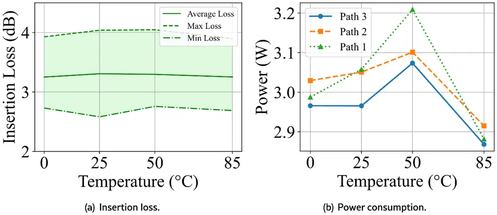
The transceiver (hardware prototype). Switching took 60–80 µs in hardware; protocol reconnection comes on top. MEMS, piezo and robotic OCSes take milliseconds to minutes. Insertion loss of the switch core ranged from 2.5 to 4.0 dB, averaged 3.3 dB at 25 °C, and barely moved from 0 to 85 °C. The core drew about 3.2 W at most for any active path (the text says less than 3.2 W); the rest of the module drew 8.5 W at 8 × 112G, so the total stayed under the 12 W limit of QSFP-DD 800G. At 620 mW drive power the bit error rate was 0 at −5 °C and 25 °C; at 50 °C and 75 °C errors appeared only at very low optical modulation amplitude (OMA).
光模組(硬體原型)。硬體切換需要 60–80 µs;協定層的重新連線另計。MEMS、壓電與機械手臂式 OCS 需要毫秒到數分鐘。開關核心的插入損耗在 2.5 到 4.0 dB 之間,25 °C 時平均 3.3 dB,從 0 到 85 °C 幾乎不變。不論啟用哪條路徑,核心最多約耗 3.2 W(內文寫的是低於 3.2 W);模組其餘部分在 8 × 112G 下耗 8.5 W,所以總功耗維持在 QSFP-DD 800G 的 12 W 上限之下。驅動功率 620 mW 時,−5 °C 與 25 °C 的位元錯誤率為 0;50 °C 與 75 °C 只在光調變幅度(OMA)非常低時才出現錯誤。
What these numbers mean for one link:
這些數字對一條鏈路的意義:
| Question問題 | Calculation算式 | Result結果 |
|---|---|---|
| Light left after the average 3.3 dB平均 3.3 dB 之後剩下的光 | about half約一半 | |
| Light left after the worst 4.0 dB最差 4.0 dB 之後剩下的光 | ||
| Switch share of the module power開關占模組功耗的比例 | at most最多 | |
| Module energy per bit at 800 Gb/s800 Gb/s 下模組每位元的能量 | pJ/bit | |
| Speed against a 1 ms mirror switch與 1 ms 的鏡面開關相比 | faster更快 |
So the switch costs about half of the light and at most a quarter of the module's power. A link must have 3–4 dB of optical margin to spare; the paper does not state the reach that remains.
所以開關要付出約一半的光,以及最多四分之一的模組功耗。一條鏈路必須多出 3–4 dB 的光功率餘裕;論文沒有說明剩下的傳輸距離。
The ring (testbed). With large messages, AllReduce used 77.11% of the ring bandwidth on 16 GPUs and 77.26% on 32 GPUs, against 81.77% for an NVIDIA H100 8-GPU server without SHARP (NVIDIA's in-switch reduction). The metric reads like the bus bandwidth of nccl-tests divided by the link rate (Chapter 4, §8). It did not fall from 16 to 32 GPUs, and it stayed 4.5 points below the switched server.
環(測試平台)。大訊息時,AllReduce 在 16 顆 GPU 上用到環頻寬的 77.11%,在 32 顆上是 77.26%;未啟用 SHARP(NVIDIA 的交換器內歸約)的 NVIDIA H100 8-GPU 伺服器是 81.77%。這個指標看起來像是 nccl-tests 的 bus bandwidth 除以鏈路速率(第 4.8 節)。從 16 到 32 顆 GPU 它沒有下降,而且一直比有交換器的伺服器低 4.5 個百分點。
Not measured. The headline comparisons, GPU waste at TP-32 of 0.53% against 10.04% for NVL-72 and 3.37× the MFU of 8-GPU nodes (only at 131,072 GPUs), are simulations driven by the trace, and this page does not show them. The claim that the interconnect costs 31% of NVL-72 comes from the paper's cost model, which prices parts from retail lists with a 60% discount: $3.28 against $10.63 per GB/s of per-GPU bandwidth for (Table 6).
沒有量測的部分。標題上的比較——TP-32 時 GPU 浪費 0.53% 對 NVL-72 的 10.04%,以及 MFU 為 8-GPU 節點的 3.37 倍(只在 131,072 顆 GPU 時)——都是以這份紀錄驅動的模擬,本頁不呈現。互連成本只有 NVL-72 的 31% 這個說法來自論文的成本模型:以零售價打六折估算零件, 時每 GB/s 的每 GPU 頻寬為 $3.28,NVL-72 為 $10.63(Table 6)。
6. Limits and open questions6. 限制與未解的問題
- Rings only. AllToAll for expert parallelism costs on a ring. Appendix G rewires backups to for Binary Exchange in , but that needs GPU forwarding, couples the TP and EP sizes, and has not run on hardware. The case that TP beats EP for MoE rests on a simulated 8-expert model with an assumed 20% imbalance.只有環。專家平行的 AllToAll 在環上要 。附錄 G 把備援改接到 ,以 Binary Exchange 做到 ,但這需要 GPU 轉送、把 TP 與 EP 的大小綁在一起,而且沒有在硬體上跑過。「MoE 用 TP 勝過 EP」的論點,建立在一個 8 個專家、假設 20% 不平衡的模擬模型上。
- No end-to-end bypass. The 32-GPU ring used fixed optics, and the 60–80 µs excludes the control plane. No measurement shows a running job surviving a node failure through OCSTrx.沒有端到端的繞過展示。32-GPU 的環用的是固定光模組,60–80 µs 也不含控制平面。沒有任何量測顯示執行中的任務透過 OCSTrx 撐過節點故障。
- Independent faults. The bound and the 4-GPU conversion assume independent GPU faults; failures that take out neighbours together would cut the line more often than predicts. The wiring may help, because HBD neighbours sit under different ToRs, but the paper does not test this.故障獨立的假設。上限與 4-GPU 換算都假設 GPU 故障獨立;會同時帶走鄰居的故障,切斷這條線的頻率會比 預測的高。接線方式也許有幫助,因為 HBD 鄰居在不同的 ToR 之下,但論文沒有測試這一點。
- Unlike fabrics. NVL-72 is any-to-any and can reduce inside the switch; InfiniteHBD is ring-only, so a cost per GB/s compares unlike things. The paper also reports about 13% lower small-message latency than "the NVLink switch design", but names neither the GPUs nor the setup, so this page does not use it.不同性質的互連。NVL-72 是任意對任意、能在交換器內歸約;InfiniteHBD 只有環,所以每 GB/s 的成本比較的是不同的東西。論文也報告小訊息延遲比「NVLink 交換器設計」低約 13%,但既沒說明 GPU 也沒說明設定,所以本頁不使用它。
- One job, one dimension. One job owns the ring and only TP uses it; both proposed ways to add dimensions give something up.一個任務、一個維度。一個任務獨占這個環,而且只有 TP 使用它;論文提出的兩種增加維度的方式都要犧牲一些東西。
7. How it connects7. 與其他內容的關聯
- Chapter 2: §01 and §02 put TP on the NVLink rung of one server; this paper stretches that rung into a datacenter-wide ring. §05 counts optics as passive parts that cost and fail; here an optic gains a switch and stays within the QSFP-DD 800G power limit (optics panel).第 2 章:§01 與 §02 把 TP 放在單台伺服器的 NVLink 這一階;這篇論文把這一階拉長成整個資料中心的環。§05 把光學元件當成要花錢、會壞的被動零件;這裡光模組多了一個開關,仍符合 QSFP-DD 800G 的功耗上限(光學面板)。
- Chapter 6, §5, and the TPUv4 resiliency digest: the same idea, rewiring around faults, done by central MEMS switches in milliseconds per cube. §4 of that chapter buys redundancy with spare ports and hosts; the K-hop ring buys it with spare fibres.第 6.9 節 與 TPUv4 韌性導讀:同樣是繞過故障重新接線,但由集中式 MEMS 開關以毫秒、以 cube 為單位完成。該第 2.5 節 用備用埠與主機買備援;K 跳環用備用光纖買備援。
- Chapter 4, §3 and §8: the ring AllReduce this HBD is built for, and busbw. Chapter 10, §5: fault radius as a design lever.第 4.2 節 與 §8:這個 HBD 為之設計的環狀 AllReduce,以及 busbw。第 10.5 節:把故障半徑當成設計槓桿。
- Guided readings: TPU v4 (cubes and OCS), Rail-only (TP is most of the bytes) and Alibaba HPN (backup hosts). FabricPerf, the first digest of this chapter, measures the switch-centric NVLink domains that this paper argues against.論文導讀:TPU v4(cube 與 OCS)、Rail-only(TP 占了大部分位元組)與 Alibaba HPN(備用主機)。本第 2 章的第一篇導讀 FabricPerf,量測的正是這篇論文所反對的、以交換器為核心的 NVLink 域。
Key numbers關鍵數字
| Number | 數字 | Meaning | 意義 | Setup | 設定 |
|---|---|---|---|---|---|
| 60–80 µs | OCSTrx switching time, hardware only | OCSTrx 切換時間,只計硬體 | Hardware prototype | 硬體原型 | |
| 2.5–4.0 dB; 3.3 dB | Insertion loss of the switch core, 0–85 °C; average at 25 °C | 開關核心的插入損耗,0–85 °C;25 °C 時的平均 | Hardware prototype | 硬體原型 | |
| ≈ 3.2 W / 8.5 W / < 12 W | Switch core at most / rest of the module / whole module | 開關核心最多 / 模組其餘部分 / 整個模組 | Hardware prototype, 8 × 112G | 硬體原型,8 × 112G | |
| 0 | Bit error rate at −5 °C and 25 °C | −5 °C 與 25 °C 的位元錯誤率 | Hardware prototype, 620 mW drive | 硬體原型,620 mW 驅動 | |
| 77.11% / 77.26% / 81.77% | AllReduce share of ring bandwidth: 16 GPUs / 32 GPUs / H100 8-GPU server without SHARP | AllReduce 用到的環頻寬比例:16 顆 / 32 顆 GPU / 未啟用 SHARP 的 H100 8-GPU 伺服器 | Testbed, fixed optics | 測試平台,固定光模組 | |
| 2.33% / 1.67% / 7.22% | Faulty 8-GPU nodes: mean / median / p99 | 故障的 8-GPU 節點:平均 / 中位數 / p99 | Production, about 3K GPUs, 348 days | 生產環境,約 3K 顆 GPU,348 天 | |
| 0.29% / 1.17% | Per-GPU fault probability; 4-GPU node rate | 每顆 GPU 的故障機率;4-GPU 節點的故障率 | Derived from the trace, independent faults | 由紀錄推得,假設故障獨立 | |
| 0.28% / 1.81% | Waste bound at p99, , TP-32: 4-GPU / 8-GPU nodes | p99、、TP-32 的浪費上限:4-GPU / 8-GPU 節點 | Analysis, Appendix C | 分析,附錄 C | |
| 30 vs 14 | Idle GPUs: two 32-GPU HBDs vs one 64-GPU HBD, two failures, TP-16 | 閒置 GPU:兩個 32-GPU HBD 對一個 64-GPU HBD,兩顆故障,TP-16 | Analysis, §1 | 分析,§1 |
Terms used on this page本頁用到的術語
- HBD (high-bandwidth domain)HBD(高頻寬域)
- The scale-up network that gives each GPU terabits per second for TP and EP, such as NVLink with NVSwitch.
- 給每顆 GPU 每秒數 Tb、承載 TP 與 EP 的 scale-up 網路,例如 NVLink 加 NVSwitch。
- Fault explosion radius故障爆炸半徑
- The number of GPUs that one fault degrades.
- 一次故障拖累的 GPU 數量。
- GPU waste ratioGPU 浪費比例
- Healthy GPUs that no group can use, as a share of all GPUs.
- 沒有任何群組能用的健康 GPU 占全部 GPU 的比例。
- OCS
- Optical circuit switching: steering light from one fibre to another without turning it into packets.
- 光路交換:把光從一條光纖導到另一條,不轉成封包。
- OCSTrx
- The paper's 800G transceiver with a built-in switch: main fibre, backup fibre or loopback.
- 論文中內建開關的 800G 光模組:主光纖、備援光纖或迴環。
- MZI
- Mach–Zehnder interferometer: two light arms whose phase difference picks the output port.
- 馬赫–曾德干涉儀:兩條光臂,其相位差決定光從哪個埠輸出。
- Insertion loss插入損耗
- Optical power lost in the switch, in dB; 3 dB is about half.
- 光通過開關時損失的功率,以 dB 計;3 dB 約為一半。
- K-hop ringK 跳環
- Each node is wired to the nodes at ; two links are active, are backups.
- 每個節點接到 位置的節點;兩條鏈路啟用, 條備援。
- Loopback path迴環路徑
- Path 3 of OCSTrx: returns the light to the other half of the lanes and closes a ring at the end of a line.
- OCSTrx 的路徑 3:把光送回另一半 lane,在一條線的末端把環閉合。
- Parallel sub-line平行子線
- The chain of nodes with the same index under consecutive ToRs; TP groups are cut along it.
- 相鄰各台 ToR 下同一編號節點串成的鏈;TP 群組沿著它切出。
- SHARP
- NVIDIA's reduction inside the switch; the 81.77% baseline ran without it.
- NVIDIA 在交換器內做的歸約;81.77% 的基準沒有使用它。